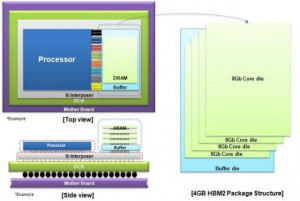

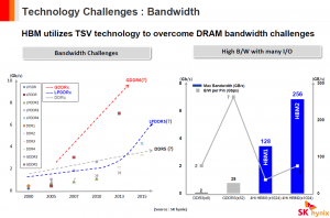
According to An And Tech, Samsung’s new high-bandwidth memory (HBM) technology will “substantially increase bandwidth available to computing devices (GPUs) and reduce power consumption”. This is the second generation of HBM, as the first (found in AMD’s Fury graphics cards) had some issues related to actual capacity and clock-rates. These new HBM2 stacks are based on the 20nm architecture, and offer twice the gigabytes per second, 256GB/s, that the first generation of HBM allowed (first gen HBM allowed for just 128GB/s). Moreover, current HBM-equipped GPUs will be able to hold as much as 16GB memory, a huge advantage over the 4GB shown in AMD’s version of the process. Getting even more technical, Samsung’s device consists of four 8Gb chips (or 4GB stacks total), which, with said 256GB/s of bandwidth, attach to the 1024-bit interface at 1.2 volts. The company is already planning on producing its own 8GB stacks, based on the notion that stacks can be two, four, or eight chips high (Ars Technica).

Despite the fact that this is an incredibly brand-new solution, Samsung obviously wants to be ahead of the pack by diving right in. Soon, we will see HBM2 technology used by graphics card makers all over, as well as big supercomputer and data centers; and smartphones and tablets will surely enjoy the amount of space saving we’re talking about. Samsung may be the first to come out and shout their plan from the rooftops (they are already in mass production), but to no surprise, AMD is already on it (as far as updating its current HBM devices), and Intel is surely expected to integrate the technology on their own chips.

 Laptop & Tablet Parts